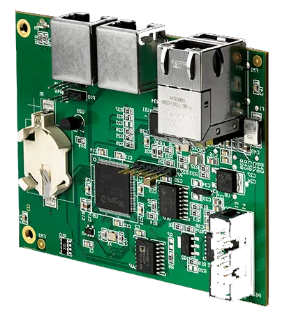
High-Volume Micro PCB Manufacturing

Sierra has spent a lot of resources in the past few years to develop our micro PCB section. Our modern facility is equipped with the best machines and engineering teams to build your microelectronics.

Email Us for a Quote

Thinking big for your micro PCB

It is crucial to address some of the causes pushing businesses towards the miniaturization of their electronics products in order to properly understand their advantages.

Consumer demand may be the most important factor in this situation. Consider how cellular phones have changed over the past 20 years, going from huge gadgets with simple functions to compact smartphones that can almost do everything. Tablets, laptops, wearables, and whatnots all follow the same pattern.

Then comes the medical industry with its demands for extra small circuits that can enhance and even save the lives of patients. Wristbands, pacemakers, neural probes, camera modules, stimulators, implants… These medtech devices mark an evolution in the healthcare system that now offers more personalized prevention and treatments.

So what are the challenges of microelectronics?

Not only do circuit boards get smaller but they also get denser. For designers, this means packing more input/output on considerably small spaces. A tighter pitch requires very fine trace and space that must meet signal integrity requirements. Of course, as your trace becomes smaller, you want to avoid losing your signal’s energy as subtractive PCB printing techniques at the microscale makes it extremely difficult to guarantee homogeneous traces.

To prevent serious electrical issues and potential failure, designers must reach out to their PCB house to learn about their capabilities. And work hand-in-hand for the best results possible.

Capabilites Overview

  • Up to 30 layers
  • Board thickness: .005″
  • Core thickness: .002”
  • Conductive filled vias
  • Edge plating
  • Bevel
  • Countersink

Special Micro features

  • Blind, buried and microvias
  • Stacked vias
  • Up to 5 sequential
  • laminations
  • High-signal performance
  • Considerations
  • Laser direct imaging

Certifications

  • ITAR
  • IPC 6012 class 1, 2 & 3
  • AS9100D
  • NADCAP
  • MIL-PRF-55110
  • MIL-PRF-31032/1
  • MIL-PRF-31032/2 
  • ISO 9001:2015
Attributes of microelectronics PCBs
PCB Attribute Sierra Circuits capability
Min Layer Count 1
Max Layer Count 30
Min Board Thickness .005″ (.127 mm)
Max Board Thickness .250″ (6.35 mm)
Min Core Thickness .002″ (.051 mm)
Min Dielectric .002″ (.051 mm)
Min Starting Copper Foil Weight 3 micron (.003 mm)
Max Finished Copper Thickness (O/L) .0015″ (.038 mm)
Max Finished Copper Thickness (I/L) .001″ (.025 mm)
Min Panel Size 12″ x 18″ (30 x 46 cm)
Max Panel Size 12″ x 18″ (30 x 46 cm) 1
Smallest Mechanical Drill Diameter .005″ (.127 mm)
Smallest Laser Drill Diameter .0025″ (.064 mm)
Min Finished Hole Size Min Finished Hole Size
Max Through Hole Aspect Ratio > 10:1
Max Blind Via Aspect Ratio .8:1
Blind Via Finished Hole Size Plated shut
Buried Via Finished Hole Size .002″ (.051 mm)
Min Trace and Space .0015″ (.038 mm)
Min Pad Size for Test .003″ (.076 mm)
Process Pad Diameter D + .004″ (.102 mm)
Stacked Vias Yes
Min Wire Bond Pad Size .0025″ (.064 mm)
Controlled Impedance Tolerance 5%
Solder Mask Registration .001″ (.025 mm)
Solder Mask Feature Tolerance .0005″ (.013 mm)
Solder Mask Min Dam Size .003″ (.076 mm)
Min Diameter Route Cutter Available .021″ (.533 mm)
Routed Part Size Tolerance .002″ (.051 mm)
Laser Hole Location Tolerance .0005″ (.013 mm)
Laser Routed Part Size Tolerance – Can only be done with panels < .032” thick .001″ (.025 mm)
Bow and Twist Tolerance Per IPC spec
Thickness Tolerance 5%
Sequential Laminations > 5 lam cycles
Buried Vias Yes
Blind Vias Yes
Conductive Filled Vias Yes – Cu plate shut
Non Conductive Filled Vias Yes
Surface finishes for microelectronics PCBs
Surface Finish Type Sierra Circuits capability
HASL (Vertical or Horizontal) No
Lead Free HASL No
OSP (Shikoku F2) Yes
OSP (Entek) Yes
ENIG (Electroless Nickel/Immersion Gold) Yes
Immersion Silver No
Electrolytic Soft Gold Yes
Electrolytic Hard Gold Yes
Selective Gold Yes
Solder mask finishes for microelectronics PCBs
Mask Finish Type Sierra Circuits capability
Semi – Glossy Yes
Glossy Yes
Matte Yes
Solder mask colors for microelectronics PCBs
Mask Color Sierra Circuits capability
Green Yes
Black Yes
Red Yes
Blue Yes
Yellow No
White No
Clear Yes
Bright White No
Purple No
Legend colors for microelectronics PCBs
Legend Color Sierra Circuits capability
All Colors Yes
Fabrication techniques for microelectronics PCBs
Fabrication Technique Sierra Circuits capability
Routed Array Yes
V Score, Edge to Copper .007″ (.178 mm)
V Score Angles 35°, 45°, 60°
Countersink Yes
Counterbore Yes
Bevel Yes
Milling +/- .003” (.076 mm)
Edge Castellation Yes
Edge Plating Yes
Heatsinks No
Electrical testing for microelectronics PCBs
Test Type Sierra Circuits capability
10 Volt Yes
40 Volt (Burn-In Boards) Yes
250 Volt Yes
500 Volt Yes
Hi Pot Yes
Laminate materials for microelectronics PCBs
Material Type Sierra Circuits capability
Very Thin Film Yes
Arlon 85NT No
Bergquist No
Hybrid Constructions Yes
Isola FR406 Yes
Isola FR408 HR Yes
Isola P95 Yes
Isola P96 Yes
Iteq IT180 Yes
Panasonic R1766 Yes
Panasonic R1755 no
Panasonic Megtron No
Nelco N4000-13 Yes
Nelco N4000-29 No
Nelco BT N5000 Yes
Nelco N7000-2 Yes
No Flow Prepreg Yes
Isola 370HR Yes
Polyclad Getek Yes
PSA Bond Film Yes
Rogers 3000 Series No
Rogers R4000 Series No
Rogers 5000 Series No
Rogers 6000 Series No
Rogers TMM No
Testing reports for microelectronics PCBs
Available Reports Sierra Circuits capability
Microsection Yes
Solderability Yes
X-Ray Fluorescence Yes
Ionic Contamination Yes
Time Domain Reflectometry Test (TDR) Yes
FAI Yes
Certificate of Compliance Yes
UL certification for microelectronics PCBs
Certification Sierra Circuits capability
94VO No
Classifications for microelectronics mil-spec PCBs
Classification Sierra Circuits capability
MIL-PRF-55110 No
MIL-PRF-31032/1 No
MIL-PRF-31032/2 No
IPC 6012, Class 1, 2 and 3 Yes
ISO 9001:2015 Yes
ISO 13485:2016 Yes