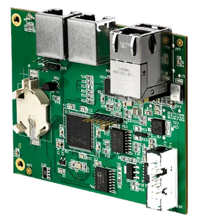
The rise in demand for compact devices where the form factor is a major concern has led to the increase in manufacturing high-density interconnects. These boards are a part of your lifestyle gadgets like wearables, smartphones, and life-saving medtech equipment.
Fabricating HDI PCBs is a challenging task as it includes fine line width (less than 4 mils), thin dielectrics, controlled impedance, blind, buried, and microvias. These features allow devices to shrink in size. This miniaturization trend has challenged manufacturers to fit more functionalities into tiny board areas.
HDI boards should be designed to maximize component density, provide efficient breakout/fanout for ICs, and transmit high-frequency signals without reflections. The ultimate goal is to integrate greater capabilities into a small package. Some of the ways of achieving this include reducing the trace width and size of the vias. This eventually increases the routing area, thereby reducing the required number of layers and the overall size of the board.
Microvias and buried vias are incorporated into circuit boards using a technique called sequential lamination. It involves building up the PCB sequentially by laminating the subparts composed of copper and dielectric layers. One of the major challenges in this process is limiting the number of lamination cycles.
The advancement of HDI technologies has now made its way to microelectronics, where fine lines, less than 1.5 mils, can be additively placed on PCBs. In contrast, traces on the conventional high-density interconnects are formed using a subtractive process (etching of copper).
As a designer, it is very important to optimize your design based on your manufacturer’s capabilities. Adhering to the guidelines of your fab house can greatly reduce the product turn time and cost.
The fabrication of HDI boards demands skilled teams and cutting edge technologies, such as sequential lamination, laser drills, and laser direct imaging. In addition to this, your coordination with your CM plays an important role to build an efficient and reliable product.
Via Type | Via parameter | Sierra Circuits capability |
---|---|---|
Blind Via | Min total pad size | 4 mils (.102 mm) over drill size |
Min laser drill size | 4 mils (.102 mm) | |
Mechanically drilled annular ring | 4 mils (.102 mm) over drill size | |
Dielectric material thickness | 2 mils (.051 mm) | |
Capture pad size | 4 mils (.102 mm) over drill size | |
Laser aspect ratio | .75:1 | |
Buried Via | Min total pad size | 5 mils (.127 mm) over drill size |
Min drill size | 6 mils (.152 mm) – depending on aspect ration | |
Capture pad size | 5 mils (.127 mm) over drill size | |
Laser aspect ratio | .75:1 | |
Through Hole | Min total pad size | 5 mils (.127 mm) over drill size |
Min drill size | 6 mils (.152 mm) | |
Capture pad size | 5 mils (.127 mm) over drill size | |
Max layer count | 26+ | |
Min finish thickness | .01″ (.254 mm) | |
Min trace width (I/L) | 3 mils (.076 mm) | |
Min trace width (O/L) | 3 mils (.076 mm) | |
Min space width (I/L) | 3 mils (.076 mm) | |
Min space width (O/L) | 3 mils (.076 mm) | |
Max lamination cycles | 4 | |
Min hole size | 6 mils (.152 mm) | |
Min pitch | .157″ (.4 mm) | |
Stacked vias | Yes | |
Staggered vias | Yes | |
Conductive filled vias | Yes | |
Non-conductive filled vias | Yes | |
Copper plate shut microvias | Yes | |
Heat sinks | Yes | |
UL 94V-0 (on selected materials) | Yes |
Report type | Sierra Circuits capability | |
---|---|---|
Specifications | IPC-6012, class 1, 2, 3, & ES | Yes |
IPC-6013, class 1, 2 & 3 | Yes | |
31032 MIL-PRF-55110 (on selected materials) | Yes | |
Reports / Certificates | Micro section | Yes |
Solderability | Yes | |
X-ray fluorescence | No | |
Ionic contamination | Yes | |
Time domain reflectometry (TDR) | Yes | |
First article inspection (FAI) | Yes | |
Certificate of compliance (C of C) | Yes | |
Electrical test | Yes |
Fabrication parameter | Sierra Circuits capability | |
---|---|---|
Panel sizes | 14×26″ (36×66 cm), 21×25″ (53×64 cm), 21x 29″ (53×74 cm), 12×18″ (30×46 cm), 18×24″ (46×61 cm), 16×18″ (41×46 cm) | |
Min board thickness | .007″ (.178 mm) | |
Max board thickness | .25″ (6.4 mm) | |
Thickness tolerance | <10% | |
Bow & twist tolerance | < 7% | |
Min core thickness | .002″ (0.51 mm) | |
Min dielectric | .002″ (.051 mm) | |
Min starting copper foil weight | 9 micron (.009 mm) |
Material Type | Raw board manufacturer | Sierra Circuits capability |
---|---|---|
FR-4 Lead Free | Isola 370 HR | Yes |
Ventec VT47 | Yes | |
Nan Ya NPG-170 | Yes | |
Polyimide | Isola P95 | Yes |
Nelco N7000-2 HT | Yes | |
Arlon 85N | Yes | |
Highspeed FR/MW Applications | Isola I-speed | Yes |
FR 408HRR | Yes | |
Nelco N4000-13 | Yes | |
Nelco N4800-20 | Yes | |
Teflon | Nelco N9000-13 RF | Yes |
Rogers RO3000 Series | Yes | |
Rogers RT/DUROID Series | Yes | |
Rogers ULTRALAM 2000 | Yes | |
Ceramic | Rogers RO4003 | Yes |
Rogers RO4350 | Yes | |
Rogers TTM 3, 4, 6, 10, 10i | Yes | |
Taconics CER-10 | Yes | |
Taconics RF-35, RF-35A2 | Yes | |
Taconics RF-60 | Yes | |
Flex | DuPont Pyralux AP | Yes |
DuPont Pyralux LF | Yes | |
DuPont Pyralux FR | Yes | |
Rigid | Laird IMPCB | Yes |
Drill parameter | Sierra Circuits capability | |
---|---|---|
Smallest laser drill diameter | .003″ (.076 mm) | |
Largest laser drill diameter | .010″ (.254 mm) | |
Max laser aspect ratio | >.75:1 | |
Min mechanical diameter | .005″ (.127 mm) | |
Max mechanical aspect ratio | > 10:1 | |
Min mechanical drill to copper | .005″ (.127 mm) | |
Min plated through hole tolerance | +/- .002” (.051 mm) | |
Min non plated through hole tolerance | +/- .001” (.025 mm) |
Board Type | Placement | Sierra Circuits capability |
---|---|---|
Rigid | Inner layer | Drill + .008″ (.203 mm) + class 2 |
Outer layer | Drill + .006″ (.152 mm) + class 2 | |
Flex | Inner layer | Drill + .010″ (.254 mm) + class 2 |
Outer layer | Drill + .008″ (.203 mm) + class 2 |
Feature | Conductor parameter | Sierra Circuits capability |
---|---|---|
Pad Size | Min pad size for electrical test | .004″ (.102 mm) |
Min wire bond pad size | .004″ (.102 mm) | |
Min Trace Vs Copper Thickness Note: Thickness includes starting foil plus panel plates (for wrap if any) to beetched. | 5 microns | .002″ (.051 mm) |
9 microns | .0025″ (.064 mm) | |
3/8 oz | .003″ (.076 mm) | |
1/2 oz | .0035″ (.089 mm) | |
1 oz | .0045″ (.114 mm) | |
2 oz | .006″ (.152 mm) | |
3 oz | .0065″ (.165 mm) | |
> 3 oz | Contact us | |
Min Space Vs Copper Thickness Note: Thickness includes starting foil plus panel plates (for wrap if any) to beetched. | 5 microns | .0025″ (.064 mm) |
9 microns | .003″ (.076 mm) | |
3/8 oz | .0035″ (.089 mm) | |
1/2 oz | .004″ (.102 mm) | |
1 oz | .005″ (.126 mm) | |
2 oz | .0065″ (.165 mm) | |
3 oz | .007″ (.178 mm) | |
> 3 oz | Contact us |
Type | Solder mask parameter | Sierra Circuits capability | |
---|---|---|---|
Liquid Photoimageable (LPI) | Colors | Green, red, blue, yellow | |
Gloss | Semi-gloss, matte (only in green) | ||
Min dam/web size SMT | .004″ (.102 mm) | ||
Min dam/web size BGA | .0035″ (0.89 mm) | ||
Clearance | >.0005″ (.013 mm) | ||
Mask-defined SMT Or BGA (not ground plane) | Yes | ||
Mask-defined features on ground plane | Yes | ||
Laser Direct Imaging (LDI) | Colors | Green, black, red, blue | |
Gloss | Semi-gloss | ||
Min web for SMT | .004″ (.102 mm) | ||
Min web for BGA | .0035″ (.089 mm) | ||
Clearance | .005″ (.126 mm) | ||
Mask-defined SMT Or BGA (not ground plane) | Yes | ||
Nelco N7000-2 | Yes | Yes | Yes |
Hi Pot | No | Yes | Yes |
No Flow Prepreg | Yes | Yes | Yes |
Panasonic Megtron | Yes | Yes | Yes |
Panasonic R1755 | Yes | Yes | No |
Panasonic R1766 | Yes | Yes | Yes |
Polyclad Getek | Yes | Yes | Yes |
PSA Bond Film | No | Yes | Yes |
Rogers 3000 Series | Yes | Yes | No |
Rogers R4000 Series | Yes | Yes | No |
Rogers 5000 Series | Yes | Yes | No |
Rogers 6000 Series | Yes | Yes | No |
Rogers TMM | Yes | Yes | No |
Ventec VT47 | Yes | No | No |
Type | Legend mask parameter | Sierra Circuits capability |
---|---|---|
Sprint | Color | White |
Min line | .050″ (1.27 mm) | |
Min height | .025″ (.635 mm) | |
Screen Printable | Colors | White, yellow, black, red |
Min line | .007″ (.178 mm) | |
Min height | .030″ (.762 mm) |
Surface finish | Sierra Circuits capability | |
---|---|---|
HASL (vertical & horizontal) | Yes | |
Lead free HASL | Yes | |
OSP (Shikoku F2 & Entek) | Yes | |
ENIG (electroless nickel / immersion gold) | Yes | |
ENEPIG (electroless nickel-electroless paladium-immersion gold) | Yes | |
Immersion silver | Yes | |
Tin nickel | No | |
Electrolytic soft gold | Yes | |
Electrolytic hard gold | Yes |
Fabrication parameter | Sierra Circuits capability | |
---|---|---|
Mechanical | Min route cutter available | .021″ (.533 mm) |
Routed part size tolerance | <.010″ (.254 mm) | |
Counter sink | Yes | |
Counter bore | Yes | |
Bevel angles | 20, 30, 45 | |
Laser | Milling, depth tolerance | +/- .003″ (.076 mm) |
Laser routed thickness | <.032″ (.813 mm) thick | |
Routed array | Yes | |
V Score | Angles | 30, 45, 60 |
Edge to copper | .007″ (.178 mm) | |
Dicing | Edge to copper | .005″ (.127 mm) |
Edge / Castellation | Min drill via | .010″ (.254 mm) |
Edge plating | Yes |
Screenable material | Sierra Circuits capability | |
---|---|---|
Carbon ink | Yes | |
Peelable solder mask | Yes |
Report type | Sierra Circuits capability | |
---|---|---|
Controlled impedance | 5% w/ F/A | |
Hi pot | Yes | |
Test voltage | 40, 250, 500 | |
Isolation resistance (Mohms) | >100 | |
>100 | <.010 | |
Min pad size | .004″ (.102 mm) |